- 您现在的位置:买卖IC网 > Sheet目录480 > MTD2955VT4 (ON Semiconductor)MOSFET P-CH 60V 12A DPAK
�� �
�
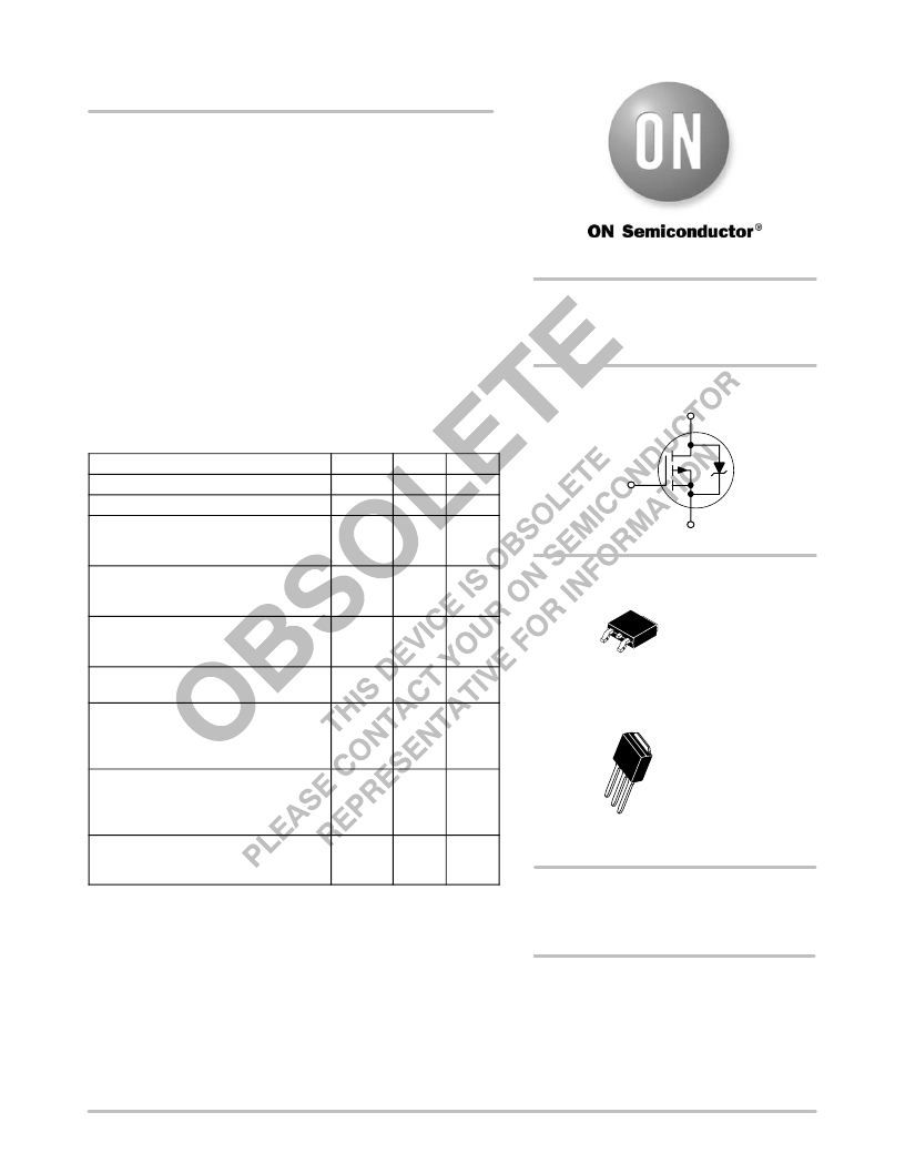
�MTD2955V�
�Power� MOSFET� 12� A,� 60� V�
�P� ?� Channel� DPAK�
�This� Power� MOSFET� is� designed� to� withstand� high� energy� in� the�
�avalanche� and� commutation� modes.� Designed� for� low� voltage,� high�
�speed� switching� applications� in� power� supplies,� converters� and� power�
�motor� controls,� these� devices� are� particularly� well� suited� for� bridge�
�circuits� where� diode� speed� and� commutating� safe� operating� areas� are�
�critical� and� offer� additional� safety� margin� against� unexpected� voltage�
�transients.�
�Features�
�?� Avalanche� Energy� Specified�
�?� I� DSS� and� V� DS(on)� Specified� at� Elevated� Temperature�
�?� Pb� ?� Free� Packages� are� Available�
�MAXIMUM� RATINGS� (T� C� =� 25� °� C� unless� otherwise� noted)�
�http://onsemi.com�
�12� A,� 60� V�
�R� DS(on)� =� 185� m� W� (Typ)�
�P� ?� Channel�
�D�
�Rating�
�Symbol�
�Value�
�Unit�
�Drain� ?� to� ?� Source� Voltage�
�Drain� ?� to� ?� Gate� Voltage� (R� GS� =� 1.0� M� W� )�
�V� DSS�
�V� DGR�
�60�
�60�
�Vdc�
�Vdc�
�G�
�Gate� ?� to� ?� Source� Voltage�
�S�
�?� Continuous�
�?� Non� ?� repetitive� (t� p� ≤� 10� ms)�
�V� GS�
�V� GSM�
�±� 20�
�±� 25�
�Vdc�
�Vpk�
�Drain� Current� ?� Continuous�
�Drain� Current� ?� Continuous� @� 100� °� C�
�Drain� Current� ?� Single� Pulse� (t� p� ≤� 10� m� s)�
�Total� Power� Dissipation�
�Derate� above� 25� °� C�
�Total� Power� Dissipation� @� 25� °� C� (Note� 2)�
�I� D�
�I� D�
�I� DM�
�P� D�
�12�
�8.0�
�42�
�60�
�0.4�
�2.1�
�Adc�
�Apk�
�Watts�
�W/� °� C�
�Watts�
�1� 2�
�3�
�4�
�DPAK� ?� 3�
�CASE� 369C�
�STYLE� 2�
�Operating� and� Storage� Temperature�
�Range�
�T� J� ,� T� stg�
�?� 55� to�
�175�
�°� C�
�Single� Pulse� Drain� ?� to� ?� Source� Avalanche�
�Energy� ?� Starting� T� J� =� 25� °� C�
�(V� DD� =� 25� Vdc,� V� GS� =� 10� Vdc,� Peak�
�I� L� =� 12� Apk,� L� =� 3.0� mH,� R� G� =� 25� W� )�
�E� AS�
�216�
�mJ�
�4�
�DPAK� ?� 3�
�Thermal� Resistance�
�?� Junction� to� Case�
�?� Junction� to� Ambient� (Note� 1)�
�?� Junction� to� Ambient� (Note� 2)�
�R� q� JC�
�R� q� JA�
�R� q� JA�
�2.5�
�100�
�71.4�
�°� C/W�
�1�
�2�
�3�
�CASE� 369D�
�STYLE� 2�
�Maximum� Lead� Temperature� for� Soldering�
�Purposes,� 1/8� ″� from� case� for� 10�
�seconds�
�T� L�
�260�
�°� C�
�Stresses� exceeding� Maximum� Ratings� may� damage� the� device.� Maximum�
�Ratings� are� stress� ratings� only.� Functional� operation� above� the� Recommended�
�Operating� Conditions� is� not� implied.� Extended� exposure� to� stresses� above� the�
�Recommended� Operating� Conditions� may� affect� device� reliability.�
�1.� When� surface� mounted� to� an� FR4� board� using� the� minimum� recommended�
�pad� size.�
�2.� When� surface� mounted� to� an� FR4� board� using� the� 0.5� sq.in.� pad� size.�
�ORDERING� INFORMATION�
�See� detailed� ordering� and� shipping� information� in� the�
�package� dimensions� section� on� page� 7� of� this� data� sheet.�
�DEVICE� MARKING� INFORMATION�
�See� general� marking� information� in� the� device� marking�
�section� on� page� 7� of� this� data� sheet.�
�?� Semiconductor� Components� Industries,� LLC,� 2006�
�August,� 2006� ?� Rev.� 8�
�1�
�Publication� Order� Number:�
�MTD2955V/D�
�发布紧急采购,3分钟左右您将得到回复。
相关PDF资料
MTD3010N
PHOTO DIODE 900NM DOME CLR TO-18
MTD3010PM
PHOTO DIODE 900NM DOME CLR TO-18
MTD3055VL
MOSFET N-CH 60V 12A DPAK
MTD3055V
MOSFET N-CH 60V 12A DPAK
MTD5010N
PHOTO DIODE 850NM DOME CLR TO-18
MTD5010W
PHOTO DIODE 850NM FLAT CLR TO-18
MTD5052N
PHOTO DIODE 525NM B/G CLR TO-18
MTD5052W
PHOTO DIODE 525NM FLAT CLR TO-18
相关代理商/技术参数
MTD2955VT4G
制造商:ONSEMI 制造商全称:ON Semiconductor 功能描述:Power MOSFET 12A, 60V P-Channel DPAK
MTD2N20
制造商:MOTOROLA 制造商全称:Motorola, Inc 功能描述:POWER FIELD EFFECT TRANSISTOR N-CHANNEL ENHANCEMENT-MODE SILICON GATE
MTD2N40E
制造商:ON Semiconductor 功能描述:Trans MOSFET N-CH 400V 2A 制造商:Rochester Electronics LLC 功能描述:- Bulk
MTD2N40ET4
制造商:Rochester Electronics LLC 功能描述:- Bulk
MTD2N50
制造商:MOTOROLA 制造商全称:Motorola, Inc 功能描述:POWER FIELD EFFECT TRANSISTOR N-CHANNEL ENHANCEMENT-MODE SILICON GATE DPAK FOR SURFACE MOUNT OR INSERTION MOUNT
MTD2N50E
制造商:MOTOROLA 制造商全称:Motorola, Inc 功能描述:TMOS POWER FET 2.0 AMPERES 500 VOLTS RDS(on) = 3.6 OHM
MTD2N50E1
制造商:Rochester Electronics LLC 功能描述:- Bulk
MTD3010N
功能描述:PHOTO DIODE 900NM DOME CLR TO-18 RoHS:是 类别:传感器,转换器 >> 光学 - 光电检测器 - 光电二极管 系列:- 标准包装:1 系列:- 波长:850nm 颜色 - 增强型:- 光谱范围:400nm ~ 1100nm 二极管类型:引脚 nm 下响应率:0.62 A/W @ 850nm 响应时间:5ns 电压 - (Vr)(最大):50V 电流 - 暗(标准):1nA 有效面积:1mm² 视角:150° 工作温度:-40°C ~ 100°C 封装/外壳:径向,5mm 直径(T 1 3/4) 其它名称:475-2649-6